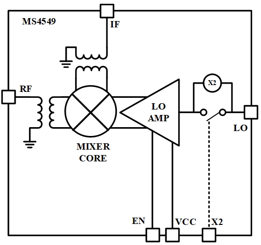
The MS4549 is a wideband RF mixer operating from 2 GHz to 15 GHz. It features an integrated on-chip balun on the IF port, providing a single-ended output that simplifies cascading with subsequent stages.
The device supports:
RF input range: 2–15 GHz
LO input range: 1–14 GHz
IF output range: 0.5–6 GHz
All ports exhibit ultra-wideband characteristics, enabling high flexibility across multiple system architectures.
The MS4549 integrates an on-chip LO amplifier, allowing operation with a typical LO drive of 0 dBm. It also includes an optional LO frequency doubler, enabling operation with lower LO frequencies and relaxing system LO source requirements.
Powered by a single 3.3 V supply, the device is easy to use and suitable for compact, low-power designs.
The MS4549 is available in both QFN package (MS4549E) and bare die form (MS4549K), with an operating temperature range from –40°C to +85°C and excellent wideband performance.
It is ideal for applications such as microwave transceivers, wireless backhaul, point-to-point communication, phased array antennas, C/X/Ku-band radar systems, test instrumentation, and satellite modems.